- Home
- About our study
About our study
Although 2D materials have attracted interest since the last century, target materials were highly limited only to Si-MOSFET and semiconductor heterostructures, and they could be fabricated only by those who have high level semiconductor technologies. In the present century, on the other hands, a variety of 2D materials are available relatively easily owing to the developments of fabrication techniques including mechanical exfoliation, CVD, and MBE. The first example was graphene, but after 2010, monolayers or multilayers of many layered materials were made, taking advantage of their weak van der Waals interlayer interactions. Our main focus is on such non-graphene 2D materials and their van der Waals heterostructures, which are fabricated by stacking various monolayer materials. With such novel 2D materials and artificial heterostructures, we are anticipating observing novel lattice structures and electronic properties which cannot be achieved in conventional bulk materials. Also, with such unique structures, we will realize unique optical and electronic devices.
Among a wide variety of research directions of 2D materials, we will focus on physical aspects and related device functions. In particular, the emphasis will be given on the following four subjects:
- (1) Growth/characterization of 2D materials and van der Waals heterostructures
- (2) Spin structures and quantum transport
- (3) Exciton physics and non-linear photonics
- (4) Functionalized devices
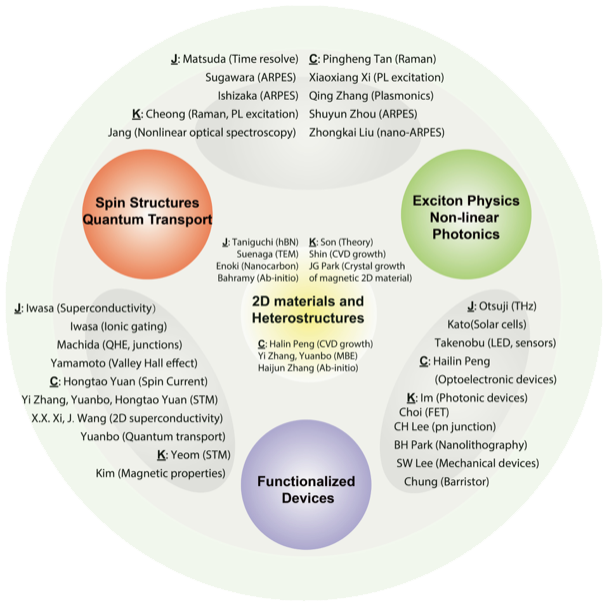
Figure 1. The research topics on 2D materials of the A3 project.